| General information | |
|---|---|
| Launched | 2019 |
| Designed by | IBM |
| Performance | |
| Max. CPU clock rate | 5.21 GHz |
| Physical specifications | |
| Cores |
|
| Cache | |
| L1 cache | 128 KB instruction 128 KB data per core |
| L2 cache | 4 MB instruction 4 MB data per core |
| L3 cache | 256 MB shared |
| Architecture and classification | |
| Technology node | 14 nm1 |
| Instruction set | z/Architecture |
| History | |
| Predecessor | z14 |
| Successor | Telum |
The z15 is a microprocessor made by IBM for their z15 mainframe computers, announced on September 12, 2019.2
Description
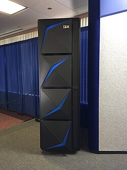
The processor unit chip (PU chip) has 12 cores. The z15 cores support two-way simultaneous multithreading.3
The cores implement the CISC z/Architecture with a superscalar, out-of-order pipeline. New in z15 is an on-chip nest accelerator unit, shared by all cores, to accelerate compression.3
The cache (e.g. level 3) is doubled from the previous generation z14, while the "L4 cache increased from 672MB to 960MB, or +43%" with the new add-on chip system controller (SC) SCM. Both it and all levels of cache in the main processor from level 1 use eDRAM, instead of the traditionally used SRAM. "A five-CPC drawer system has 4800 MB (5 x 960 MB) of shared L4 cache."
References
References
- "IBM z15 (z15)". IBM. Archived from the original on 2020-04-20.
- "IBM Unveils z15 With Industry-First Data Privacy Capabilities" (Press release). IBM. September 12, 2019. Archived from the original on 2020-01-01. Retrieved 2019-09-15.
- IBM z15 (8561) Technical Guide (PDF). September 2019. SG24-8851-00. Retrieved September 14, 2019.