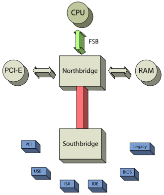
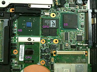
In computing, a southbridge is a component of a traditional two-part chipset architecture on motherboards, historically used in personal computers. It works alongside the northbridge to manage communications between the central processing unit (CPU) and lower-speed peripheral interfaces. The northbridge typically handled high-speed connections such as RAM and GPU interfaces, while the southbridge managed lower-speed functions.
The southbridge controls a range of input/output (I/O) functions, including USB, audio, firmware (e.g., BIOS or UEFI), storage interfaces such as SATA, NVMe, and legacy PATA, as well as buses like PCI, LPC, and SPI.12
Southbridge and northbridge components were often designed to work in pairs, though there was no universal standard for interoperability.3 In the 1990s and early 2000s, they commonly communicated via the PCI bus; more recent chipsets use Direct Media Interface (Intel) or PCI Express (AMD).
Intel referred to its southbridge as the I/O Controller Hub (ICH), later replaced by the Platform Controller Hub (PCH), which connected directly to the CPU in later architectures. Since the mid-2010s, the traditional two-chip design has largely been replaced by single-chip platforms or system-on-chip (SoC) solutions that integrate southbridge functions into a single chipset or the CPU itself.
Evolution
Single-chip platforms
Single-chip platforms has the motherboard chipset only consist of one chip. This is most commonly achieved by integrating the northbridge functionality into the CPU package or CPU die. Two examples are Intel's Sandy Bridge4 and AMD's Fusion processors,5
Intel
With the Intel 5 Series chipset in 2008, the CPU takes over the job of the northbridge. The remaining tasks of the motherboard were given to a single chip, forming the Platform Controller Hub (PCH) architecture. On Intel platforms, all southbridge features and remaining I/O functions are managed by the PCH, which is directly connected to the CPU via the Direct Media Interface (DMI).6 Intel low-power processors (Haswell-U and onward) and ultra low-power processors (Haswell-Y and onward) also integrate an on-package PCH. AMD Ryzen processors also integrated some southbridge functions, such as some USB interfaces and some SATA/NVMe interfaces.7
AMD
AMD did the merging of northbridge into the CPU with the release of their first APUs in 2011, naming the remaining singular chip (analogous to PCH) the fusion controller hub (FCH). The FCH was only used on AMD's APUs until 2017.
SoC and SiP
System on a chip processors, commonly found in mobile contexts, integrate both the south and north bridges into the CPU chip. System in package designs are similar, except the CPU package is a multi chip module (MCM) consisting of multiple chips. This improves yields in exchange for a lower degree of integration.
AMD
AMD has used an SoC design on desktop and server processors since 2015 with the Excavator Carrizo core.8 What is known as the "chipset" is instead a special PCIe device that combines the functionalities of an PCIe switch (which expands the number of available PCIe lanes), a USB host, and/or a SATA host. This device connects to the CPU via a dedicated PCIe link.9 [Non-HEDT desktop processors since Zen 2 (2019) use a MCM design with separate CPU and I/O dies (system in package).]10
Technically the processor can operate without a chipset; it only continues to be present for interfacing with low speed I/O. AMD server CPUs adopt a self contained system on chip design instead which doesn't require a chipset.11121314
Intel
Beginning with ultra-low-power Haswells and continuing with mobile Skylake processors, Intel incorporated the southbridge IO controllers into the CPU package, eliminating the PCH for a system in package (SiP) design with two dies; the larger die being the CPU die, the smaller die being the PCH die.15 Rather than DMI, these SOPs directly expose PCIe lanes, as well as SATA, USB, and HDA lines from integrated controllers, and SPI/I²C/UART/GPIO lines for sensors. Like PCH-compatible CPUs, they continue to expose DisplayPort, RAM, and SMBus lines. However, a fully integrated voltage regulator will be absent until Cannon Lake.
Etymology
The name is derived from representing the architecture in the fashion of a map and was first described as such with the introduction of the PCI Local Bus Architecture in 1991. At Intel, the authors of the PCI specification viewed the PCI local bus as being at the very centre of the PC platform architecture (i.e., at the Equator).
The northbridge extends to the north of the PCI bus backbone in support of CPU, memory/cache, and other performance-critical capabilities. Likewise the southbridge extends to the south of the PCI bus backbone and bridges to less performance-critical I/O capabilities such as the disk interface, audio, etc.
The CPU is located at the top of the map at due north. The CPU is connected to the chipset via a fast bridge (the northbridge) located north of other system devices as drawn. The northbridge is connected to the rest of the chipset via a slow bridge (the southbridge) located south of other system devices as drawn.
Although the current PC platform architecture has replaced the PCI bus backbone with faster I/O backbones, the bridge naming convention remains.
Functionality
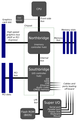
The functionality found in a 2000s southbridge includes:162
- PCI bus. A south bridge may also include support for PCI-X.
- Low speed PCI Express (PCIe) interfaces usually for Ethernet and NVMe.
- ISA bus or LPC bridge. ISA slots are no longer provided on more recent motherboards. The LPC bridge provides a data and control path to the super I/O (the normal attachment for the PS/2 keyboard and mouse, parallel port, serial port, IR port, and floppy controller).
- I2C and SMBus controller.
- DMA controller. The 8237 DMA controller allows ISA or LPC devices direct access to main memory without needing help from the CPU.
- PIC and I/O APIC.
- Mass storage interfaces such as SATA, M.2, and historical PATA. This typically allows attachment of hard drives or SSDs.
- Real-time clock.
- Programmable interval timer.
- High Precision Event Timer.
- ACPI controller or APM controller.
- SPI serial bus mostly used for firmware (e.g., BIOS/UEFI) flash storage access.
- Nonvolatile BIOS memory. The system CMOS (BIOS configuration memory), assisted by battery supplemental power, creates a limited non-volatile storage area for BIOS configuration data.
- Intel HD Audio or AC'97 sound interface.
- USB interfaces.
Optionally, a southbridge also includes support (onboard discrete chip or southbridge-integrated) for Ethernet, Wi-Fi, RAID, Thunderbolt, and Out-of-band management.
References
References
- "What is Southbridge?", Webopedia Computer Dictionary (word definition), 4 November 2002
- Mujtaba, Hassan (2019-09-13). "Intel Z490, H470 Motherboards For 10th Gen Comet Lake-S CPUs Leaked". Wccftech. Retrieved 2020-10-30.
- Chipset: Northbridge and Southbridge, Rigacci
- Vatto, Kristian. "Why Ivy Bridge is still Quad-core?". Anandtech. Archived from the original on December 7, 2011. Retrieved September 27, 2015.
- Stokes, Jon (11 November 2010). "With Fusion, AMD's devils are in the details". Arstechnica. Retrieved September 27, 2015.
- "Mobile Intel HM57 Express Chipset". Intel. Retrieved 2014-04-21.
- Hagedoorn, Hilbert (23 May 2019). "AMD Ryzen 3000: New Block diagram about PCIe 4.0 on Matisse and X570 chipset". Guru3D.com. Retrieved 2020-06-12.
- "AMD at ISSCC 2015: Carrizo and Excavator Details".
{{cite web}}: CS1 maint: deprecated archival service (link) - "AMD Zen 4 Ryzen 9 7950X and Ryzen 5 7600X Review: Retaking the High-End".
{{cite web}}: CS1 maint: deprecated archival service (link) - "Chiplets Are the Future, but They Won't Replace Moore's Law".
- "AMD Documentation Hub" (PDF). www.amd.com. Retrieved October 9, 2024.
- Kennedy, Patrick (2019-04-08). "Supermicro M11SDV-4C-LN4F Review mITX AMD EPYC 3151 Platform". ServeTheHome. Retrieved 2024-08-18.
- Cutress, Andrei Frumusanu, Dr Ian. "AMD 3rd Gen EPYC Milan Review: A Peak vs Per Core Performance Balance". www.anandtech.com. Retrieved 2024-08-18.
{{cite web}}: CS1 maint: deprecated archival service (link) CS1 maint: multiple names: authors list (link) - "The AMD Zen and Ryzen 7 Review: A Deep Dive on 1800X, 1700X and 1700". Archived from the original on March 7, 2017.
- Cutress, Ian. "Intel Releases Broadwell-U: New SKUs, up to 48 EUs and Iris 6100". www.anandtech.com. Archived from the original on January 7, 2015.
- What is a chipset?, UK: Misco.
External links
External links
- "Motherboards & Core-Logic Chipsets: The Deep Stuff > What the North Bridge and South Bridge Do". InformIT. Retrieved November 18, 2010.